A few nights back, Brian and I took some images from the SEM. We exported them into TIF format, and then copied them via Sneakernet, a.k.a. using 3.5″ floppy disks and a portable USB floppy reader. I converted them into .png files. Click them for full 1024×768 resolution, the limit of the Leica image capture board. I’m very happy with how they turned out.
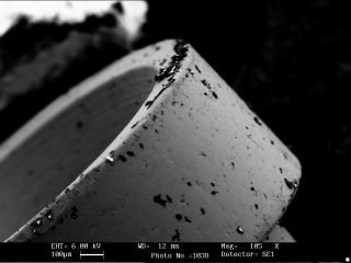
This is the top of a metallic pin or electronic contact, showing what appear to be machining marks as well as what looks like a good deal of surface contamination. Note the scale showing 100 microns.
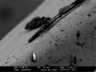
This is an enlargement of the upper rim. Note the scale showing 10 microns.
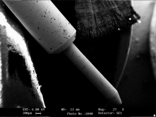
This is a lower magnification image of bottom part of the pin, as well as other items mounted on the sample stub.
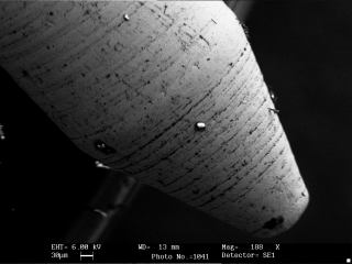
This is the point of the pin. Machining marks are clearly visible, as are surface contamination. The scale shows 30 microns.
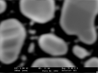
This doesn’t show much detail, and clearly has some artifacts, but look at the magnification! I believe the sample is gold sputtered onto carbon tape, and I’m guessing these are droplets of adhesive. Note the scale representing 100 nanometers. By comparison, the wavelength of visible light is 380 – 740 nanometers.
