PS:One’s scanning electron microscope came with an Oxford Isis EDX detector that we were told was non-functional. After a little poking around, I discovered that the replacement power supply which supposedly didn’t work was shipped from London, where the default power is 240V. After changing the voltage, the computer suddenly recognized the electronics, and it passed all the self tests. That looked like a good sign, so the next step was to acquire liquid nitrogen, which is needed to cool the detector.
Fortunately, one of our members owns NFC, a company that, among other things, sells liquid nitrogen. He loaned us a dewar of LN2 so we could test it out. After transporting it back to the space, I asked Everett to watch from a safe distance and let me know if anything was spilling while I filled the dewar attached to the SEM. He took some video of the process. The plastic funnel I used was cracking as I was pouring, which in hindsight wasn’t that great of an idea, so maybe we need to find another solution here….
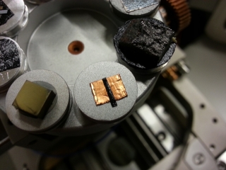
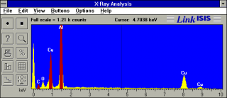
The detector took over an hour to cool down, but ultimately it worked beautifully! I kicked up the energy of the electron beam to 20 keV which excited the atoms in the sample to give off characteristic X-rays. The EDX unit measured the energy spectrum of the X-rays given off, and was able to suggest possible elements that have those peaks, which I could then label. The next day Susan Young, the microscopist who used this SEM when it was at its former home, came to the space to give me some advice on the EDX and the sputter coater. After calibrating the detector on a copper target, I then tried imaging a sample that consists of an aluminum sample stub, copper foil, and carbon tape, that has some of each of these exposed.
I’ve labeled three peaks for copper, one for aluminum, and one for oxygen. The peak at 0 is just an artifact of the detector. Here is a movie of the X-ray peaks building as the detector collects data:
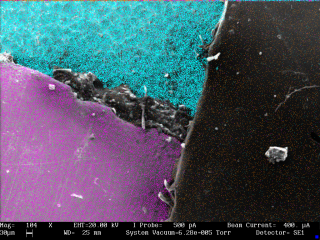
The complete spectrum is shown at the left. The EDX detector has the ability to determine not just what is in a sample, but where it occurs in the sample. I did this by defining energy windows, shown in red. One for carbon, one for one of the copper peaks, and one for aluminum. Each time an X-ray falls within one of the bands is detected, the EDX sends a pulse on one of several channels to the SEM. The SEM operates in X-ray mapping mode and, because it knows the beam’s position when the pulse is received, it makes a dot on a color coded map showing where that element occurs. This map is an overlay on the secondary electron image of the sample.
The aluminum peak is colored cyan, which dominates the upper left part of the sample. Magenta corresponds to the copper peak, which appears primarily on the lower left. Orange represents carbon. The detector didn’t detect that much of the carbon peak (seeing as it’s the smallest of the three), but orange dots are clearly visible on the right hand side. The surface in the middle is the edge of the copper tape, but it is almost vertical relative to the electron beam, so it doesn’t seem to be giving off many X-rays.
All in all, this is seriously cool technology.


